IBM Research details first sub-1 nm chip, unveils nanostack architecture
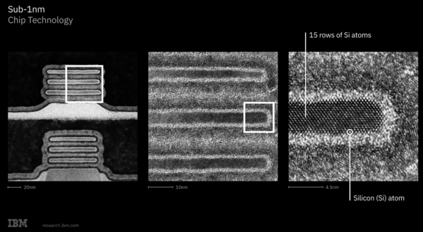
IBM said it has launched the first sub-1 nanometer (nm) chip technology with a transistor architecture at 0.7 nm. The most common chip classes for devices and AI are 3 nm to 5 nm.
According to IBM, sub-1 nm chip technology will be in production as early as five years.
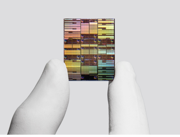
The sub-1 nm chip has nearly 100 billion transistors on a chip the size of a fingernail and has nearly twice the density of IBM's 2 nm chip that launched in 2021.
IBM said the new chip would offer up to 50% more performance and 70% more energy efficiency compared to IBM's 2 nm chips.
Jay Gambetta, Director of IBM Research, said the breakthrough came courtesy of a new nanostack architecture. IBM Research is a big part of IBM's semiconductor play. IBM recently announced it will create a quantum chip foundry called Anderon.
- IBM to invest $10 billion in quantum over 5 years
- IBM launches quantum chip foundry Anderon, lands US govt investment
- IBM delivers strong Q1, maintains outlook
Although IBM has a long history of cutting edge breakthroughs, it's unclear whether it will benefit directly from commercialization. Nevertheless, IBM sub-1 nm chip and nanostack architecture means it has "at least a decade of future scaling" ahead.
Key points about IBM's chip design.
- IBM's nanostack architecture is a 3D nanosheet-based design that was cooked up for the sub-1 nm chip.
- Nanostack vertically stacks and staggers transistors to pack more on a chip.
- IBM is using different material combinations on each stacked layer to optimize performance and power efficiency for each transistor.
- The nanostack technology has been verified and can be physically built and support computation.
- IBM researchers demonstrated that nanostack architecture provides 40% scaling in SRAM. That matters since AI workloads gobble up memory and tax data bandwidth.
More research:
Larry Dignan is Editor in Chief of Constellation Insights at Constellation Research, where he leads editorial coverage focused on enterprise technology, digital transformation, and emerging trends shaping the future of business. He oversees research-driven news, analysis, interviews, and event coverage designed to help technology buyers and vendors navigate complex markets with clarity and context. ...
Read morePublished
Author
